
Get a Quote
Please fill in the form and we will get back to you soon!
We appreciate you contacting iWave.
Our representative will get in touch with you soon!
Get in Touch
We appreciate you contacting iWave.
Our representative will get in touch with you soon!


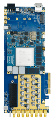
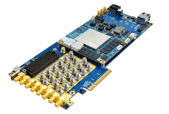
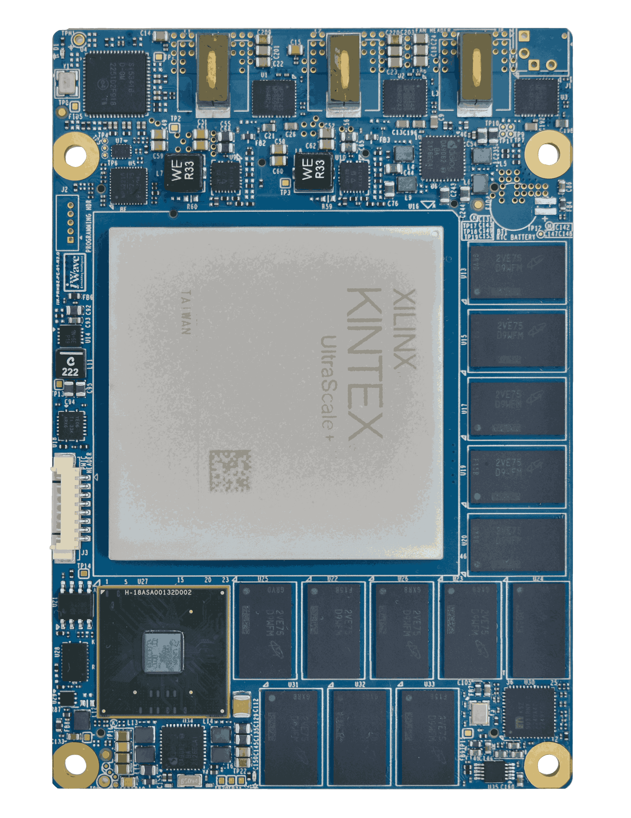
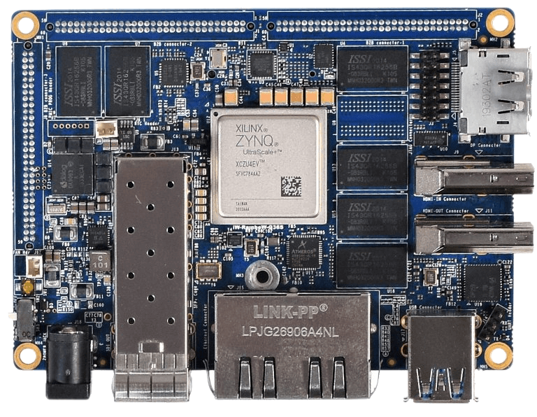
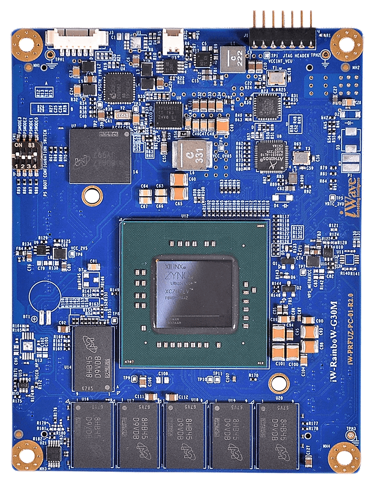
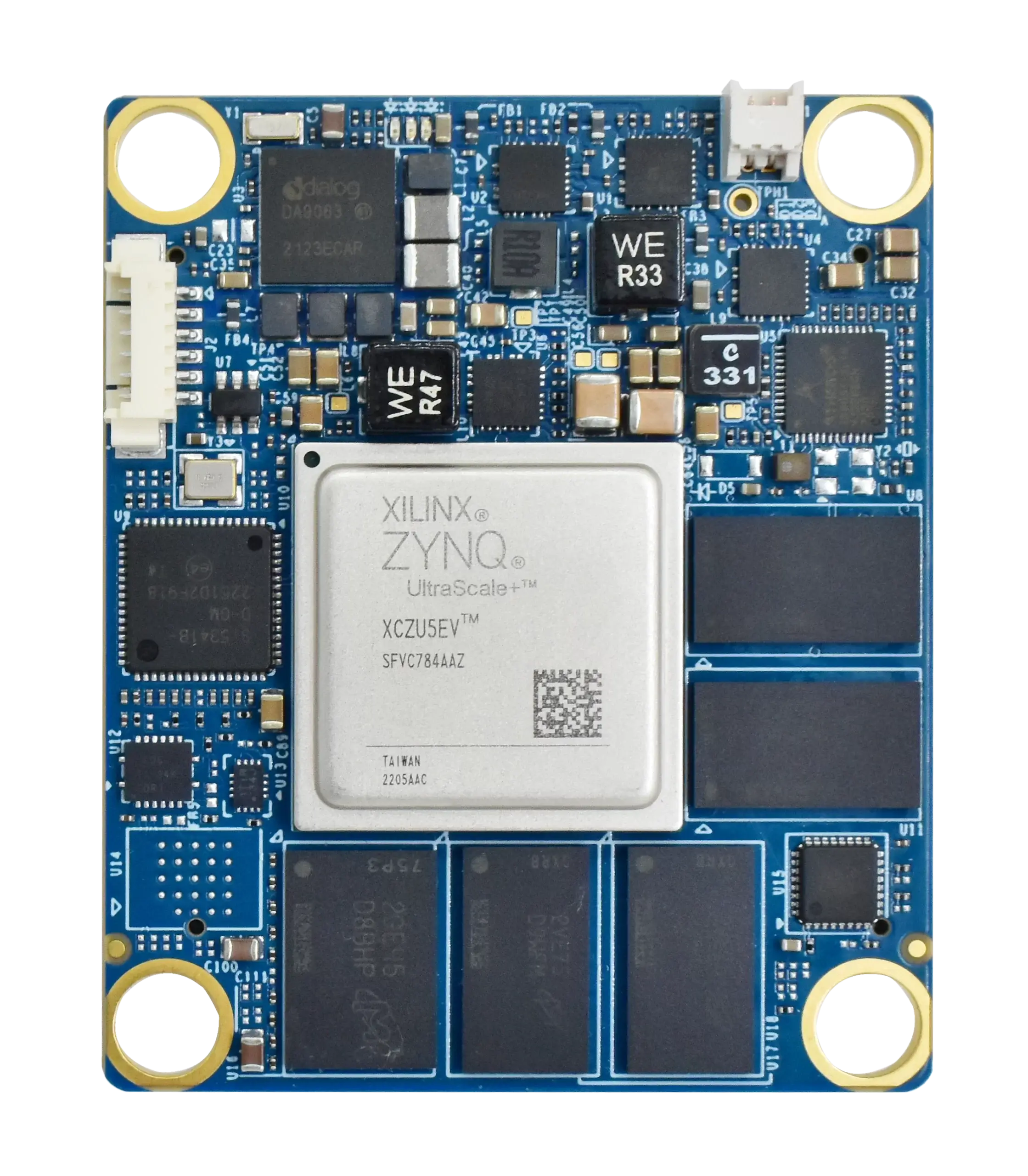
On Module Features:
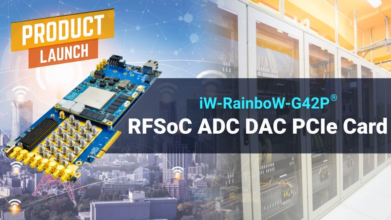
| Zynq Ultrascale+ RFSoC |
|
|---|---|
| Memory |
|
Board to Board Connector1 Interfaces (400pin):
| ADC | 16 x ADC Channels up to 2.5Gsps |
|---|---|
| DAC | 16 x DAC Channels up to 10Gsps |
| PL IOs | PL IOs – 188 IOs
|
Board to Board Connector2 Interfaces (400pin):
| From PL Block |
|
|---|---|
| From PS Block |
|
| Clock signals |
|
General Features:
| Power Input | 12V through B2B Connector2 |
|---|---|
| Form Factor | 90mm x 100mm(BRYN) |
| BSP Support | Linux BSP:- Petalinux/vivado 2022.2 |
| Operating Temperature | -40°C to +85°C (Industrial Grade) |
| Environment Specification | REACH & RoHS3 Compliant |
| Compliance | CE* |
Related products
Related products
Related News

Download
Please fill in the form below to download the document.
Thanks for filling in the download form.
Download
Please fill in the form below and we will get back to you soon!
We appreciate you contacting iWave.
Our representative will get in touch with you soon!
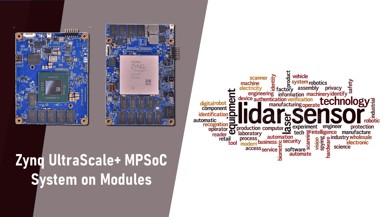
Zynq UltraScale+ RFSoC SOM
System on Module
Development kit
iWave is an embedded systems engineering and solutions company, designing solutions for the Industrial, Medical, Automotive and Avionics vertical markets, and building on our core competency of embedded expertise since 1999. Read More…