- Products
- Automotive
- Avionics
COTS Module
- Zynq RFSoC ADC DAC PCIe Card
- Agilex 7 SmartNIC Card
- ZU19/17/11 PCIe SmartNIC Card
- Kintex-7 PCIe Card
- PCIe to SD 3.0 M.2 Module
- Zynq ZU7/ZU5/ZU4 3U-VPX
- Virtex UltraScale+ 3U VPX
- Kintex UltraScale+ 3U VPX
- Zynq ZU19/17/11 3U VPX
- Kintex-7 3U VPX Card
- PCIe Gen3 x8 FMC Module
- Quad QSFP28 FMC+ Module
- PCIe Gen4 x16 FMC+ Module
- FMC Add-On Cards
- FPGA IP
- ODM Solutions
- Custom Design
- Resources
- Company


Get a Quote
Please fill in the form and we will get back to you soon!
We appreciate you contacting iWave.
Our representative will get in touch with you soon!

Get in Touch
We appreciate you contacting iWave.
Our representative will get in touch with you soon!
Thank you for subscribing to our newsletter!
Documents
Design Support
Application Notes
Software
Documents
Design Support
Application Notes
Software
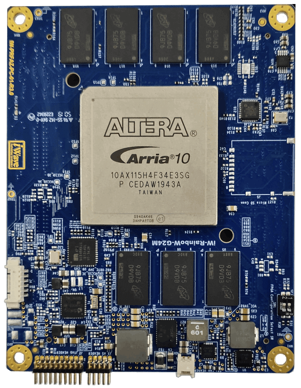
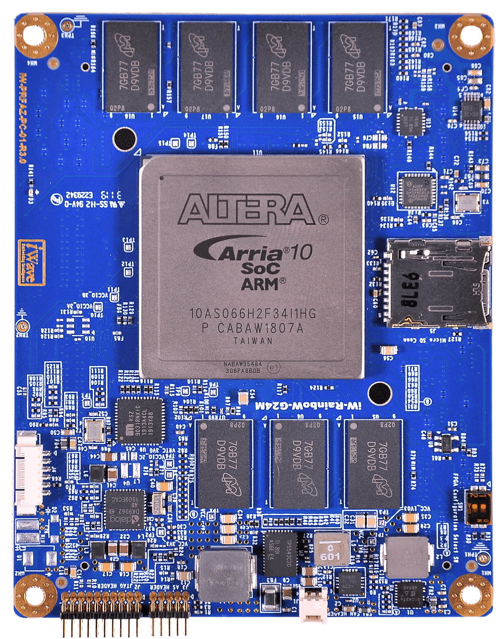
Arria 10 FPGA SOM
Arria 10 FPGA SOM
- Arria 10 FPGA device compatibility (GX270, GX320, GX480, GX570, GX660, GX900, GX1150)
- With upto 1150K Logic Elements and 24 High Speed transceivers
- 4-GB DDR4 RAM (64bit) & 2-GB DDR4 RAM for FPGA
- 24 high-speed transceivers @ 17.4Gbps
- 48/96 LVDS from BANK 3B & 3C and 93 SE from BANK 2A & 3A
- Dual 240 Pin Board to Board Connector
- Variable IO voltage support from PMIC
- Industrial Grade operation
- 10+ Years Longevity
On Module Feature:
|
Two 240pin High Speed Board to Board Connectors Interfaces
| From connector 1 interface |
|
|---|---|
| From connector 2 interface |
|
General Features:
| Power Input | 5V |
|---|---|
| Operating Temperature | -40°C to +85°C |
| Form Factor | 75mm x 95mm |
| BSP Support | Linux BSP:- Linux 5.4/Quartus 21.3 |
| Environment Specification | RoHS &REACH Compliant |
| Compliance | CE* |
DEVELOPMENT KIT – DUAL FMC
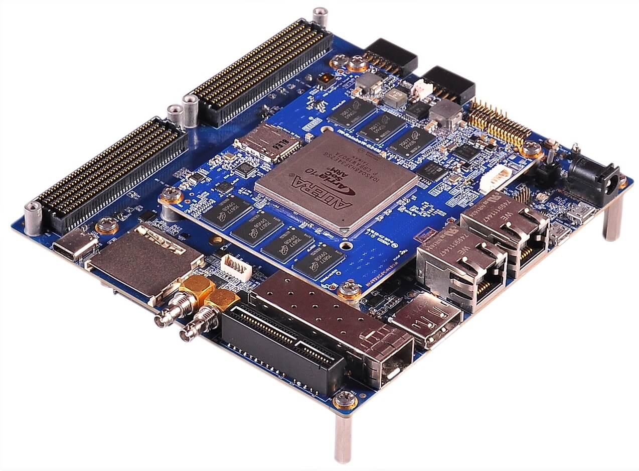
- Gigabit Ethernet through RJ45MagJack x 1
- USB2.0 OTG through Micro AB connector x 1
- Debug UART through USB Micro AB connector x 1
- 10G Ethernet through SFP+ Connector
- PCIe Gen3 x 1 Connector
- Dual PMOD Connector
- Dual FMC High Pin Count (HPC) Connector
- SDI Video IN through HD BNC Connector x 1
- SDI Video Out through HD BNC Connector x 1
- M.2 SATA Connector x 1
- USB3.0 TypeC connector x 1
- Display Port Connector x 1
- Clock Synthesizer/Generator
- 16-Bit IO Expander
JTAG Connector x 1
20 Pin GPIO Header x 1 - RTC Coin Cell Holder
Power ON/OFF DIP Switch x 1 - Reset Push button Switch x 1
- Power Supply : DC 12V, 5A Power Input Jack
- Form Factor: 130mm x 140mm
Need help with your FPGA and Product Design?
THERMAL SOLUTIONS
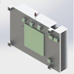
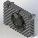
For any highly integrated System On Modules, thermal design is very important factor. iWave Supports Heat Sink and Fan Sink Solution for Arria10 SoC FPGA SOM.
Related products
RELATED VIDEOS
Related products
Related News

Download
Please fill in the form below to download the document.
Thanks for filling in the download form.

Download
Please fill in the form below and we will get back to you soon!
We appreciate you contacting iWave.
Our representative will get in touch with you soon!
Arria 10 FPGA SOM

Development Kit

Development Kit
iWave is an embedded systems engineering and solutions company, designing solutions for the Industrial, Medical, Automotive and Avionics vertical markets, and building on our core competency of embedded expertise since 1999. Read More…
Newsletter
Copyright © 2022 iWave Systems Technologies Pvt. Ltd.

