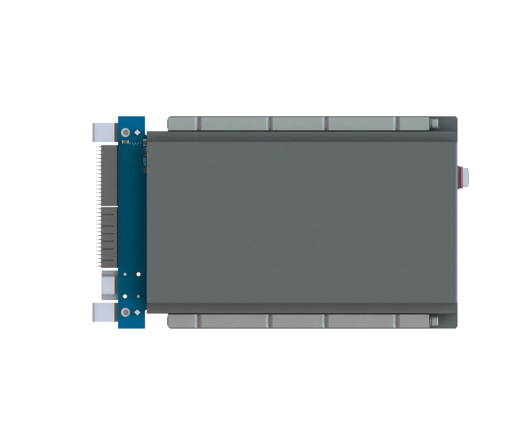
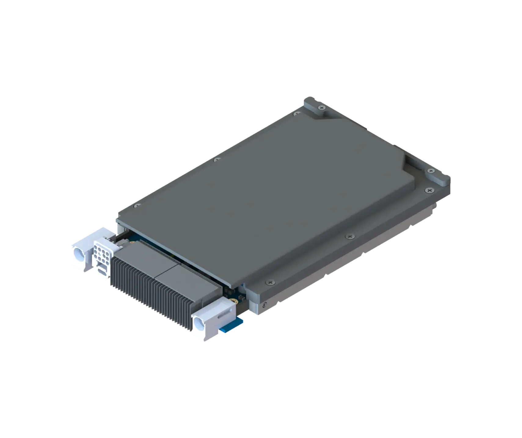
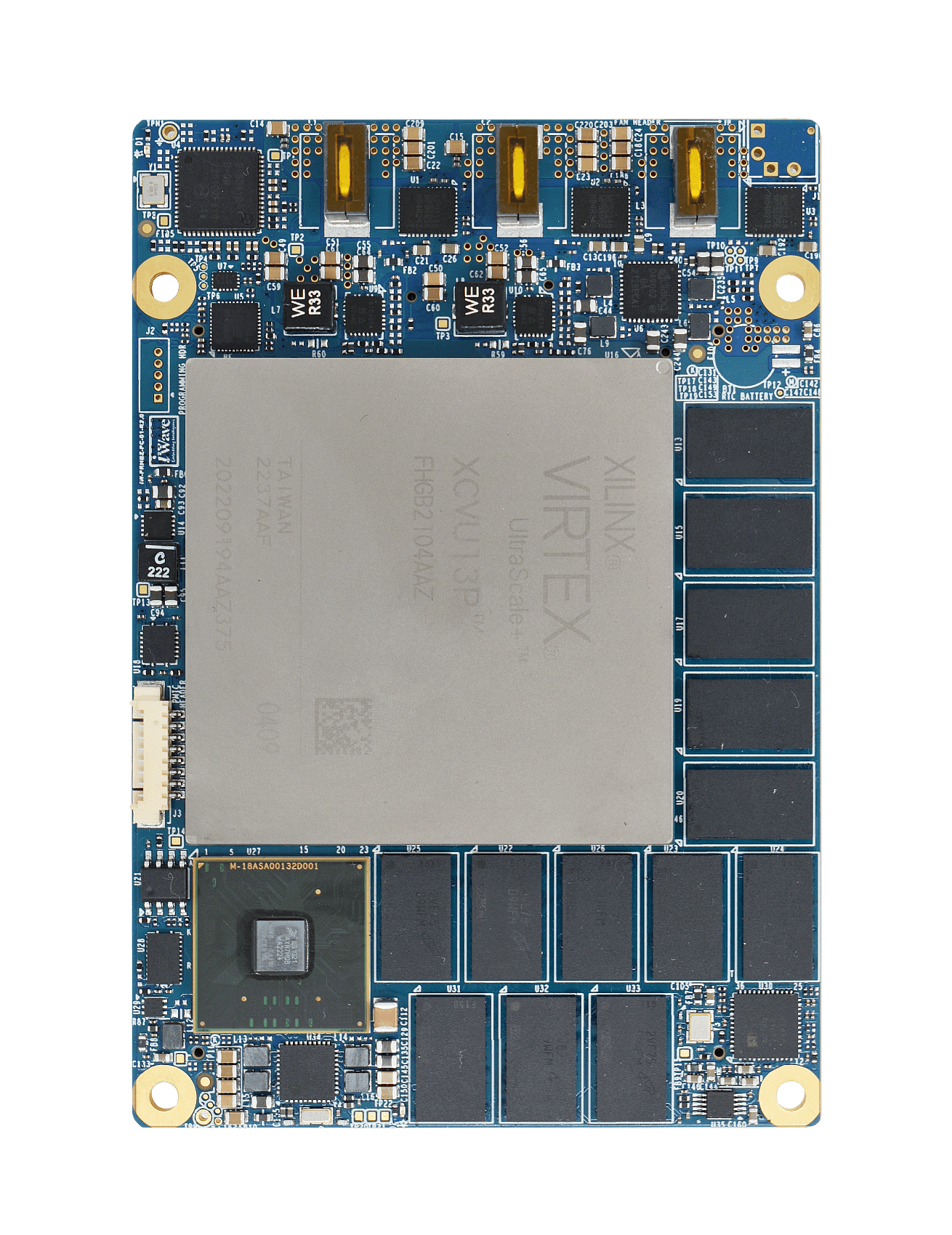
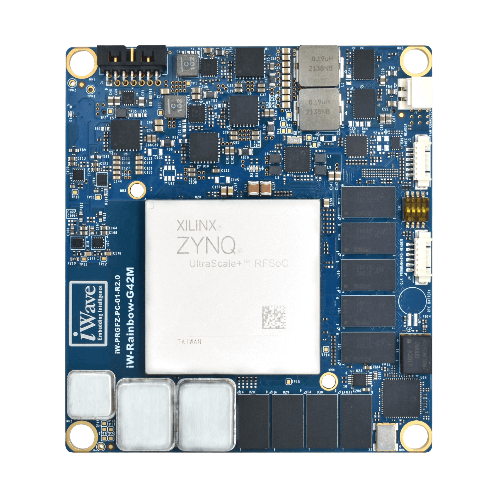
RFSoC ADC DAC 3U VPX Module

RFSoC ADC DAC 3U VPX Module

iW-RainboW-G60V

  • AMD Xilinx’s ZU48/47/43/28/27/25DR Zynq Ultrascale+ RFSoC
    • RAM Bandwidth
    • 64-bit 8GB PL DDR4 for PL
  • 64-bit 8GB PS DDR with ECC for PS
  • 8 DAC channels | 30 MHz–6 GHz | up to 9.85 GSPS
  • 8 ADC channels | 30 MHz–6 GHz | up to 5 GSPS
  • Integrated ultra low-noise programmable RF PLL
  • Integrated SyncE & PTP Network Synchronization
Categories: ,

Zynq Ultrascale+ RFSoC ZU48DR/47/43/28/27/25DR

CPU

Processing System (PS)

  • Quad-core ARM Cortex-A53 MPCore Application processor (up to 1.3GHz)
  • Dual-core ARM Cortex-R5 MPCore Real Time Processor (up to 533MHz)

Programming Logic (PL)

  • Programming Logic (PL) with up to 930K Logic cells
  • PL GTY High Speed Transceivers x 16 @ upto 28.21 Gbps
RAM Memory

64bit, 8GB DDR4 RAM for PS with ECC
64bit, 8GB DDR4 RAM for PL

Flash Memory

256MB QSPI Flash for Booting
32GB eMMC Flash for Storage
2-Kbit EEPROM x2

Clock & PLL

Integrated Configurable ultra low noise PLL for ADC & DAC
Fully Configurable Clock Synthesizer with SyncE and PTP support

3U VPX Backplane Features

3U VPX Connector (P0+P1A)
  • Data Plane Port: DP01[3:0]
    • 40GBASE-KR4 using PL GTY Bank Transceivers
  • Data Plane 1 Ultra-Thin Pipe
    • DPutp01 – 1000BASE using PL IOs. Optionally supports 10GBASE-KR using PL GTY Bank Transceivers.
  • Control Plane Ultra-Thin Pipe
    • CPutp01 – 1000BASE using PL Bank IOs. Optionally supports 10GBASE-KR using PL GTY Bank Transceivers.
  • Utility Plane
    • System Control Signals,System Reference Clocks, Bussed GPIO, Power Input (12V VDC, 3.3V_AUX,VBAT)
3U VPX Connector (P1B+P2A)
  • Expansion Port
    • PCIe Gen3 x8 using PL GTY Bank Transceivers.
  • Utility Plane
    • System Control Signals
  • Maintenance Port
    • MP01 & MP02

NanoRF +MT Ferrule Hybrid Connector -(P2B )

  • 4 DAC channels supporting 30 MHz to 6 GHz with sampling rates up to 9.85 GSPS (Configurable).
  • 4 ADC channels supporting 30 MHz to 6 GHz with sampling rates up to 5 GSPS (Configurable).
  • Multi-gigabit transceivers lanes x4 to backplane using Optical Firefly

Front Panel Features

  • USB 3.0 through USB Type-C Connector (Optionally supports DP)
  • 10/100/1000Mbps Ethernet through 9 Pin Header
  • 3 Pin Debug UART Header
  • Micro-SD Connector

Other On Board Features

  • PCIe Gen2 x2 through M.2 Connector
  • Temperature Sensor
  • Elapse Time Counter
  • Clock Synthesizer for Transceiver Reference clocks

General Specification

  • Power Input: +12VDC and 3V3_AUX input from VPX Connector
  • Thermal Solution: Integrated Heat Spreader
    Form Factor: 3U VPX (160mm X 100mm)
  • Module Profile : MOD3p-PAY-1F1U1S1S1U1U4F1J-16.6.13-n
  • Slot Profile : SLT3p-PAY-1F1U1S1S1U1U4F1J-14.6.13-n
  • Slot Pitch: 1 Inch Conduction Cooled
    Operating Temperature: -40°C to +85°C
  • Environment Specification: REACH & RoHS Compliant

Custom Design Sevices

iWave provides end-to-end ODM services, from concept to production, leveraging our in-house expertise in hardware design, software development, FPGA design, and mechanical enclosure design. The FPGA expertise at iWave includes RTL, high speed bus interface and transceivers, storage, video, networking, and high-speed ADC/DAC with the entire product lifecycle, from initial concept to mass production and ongoing support.

THERMAL SOLUTIONS

For any highly integrated FPGA VPX Plug-in Module, thermal design is a very important factor. iWave supports a VITA 65.0 compliant 3U Conduction Cooled heat spreader.

RELATED VIDEOS

Play Video about FPGA YouTube Thumbelina
Play Video about Versal AI youtube banner
Play Video about Versal AI and Versal Premium Video

Copyright © 2022 iWave Systems Technologies Pvt. Ltd.