
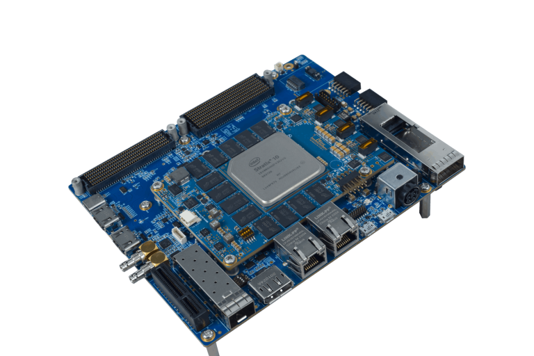
Stratix10 GX/SX SoC FPGA SOM開発プラットフォームの利用開始
開梱
箱から開発プラットフォームを取り出し、ESDフリーエリアの上に置きます。静電気防止パッド/マットを使用し、適切に接地して開発プラットフォームを設置してください。また、以下の納品物が物理的な損傷なく受け取られていることを確認してください。
開発キットの内容
- Stratix10 GX/SX SoC FPGA SOM Development Platform
- 12V, 14A Power Supply
- 安全ガイドライン
- USBデバッグケーブル
- ヒートシンク+ファン


安全ガイドライン
Stratix10 GX/SX SoC FPGA SOM Development Platform
ヒートシンク+ファン


12V, 14A Power Supply
USBデバッグケーブル
知る


Stratix10 GX/SX SoC FPGA SOM – Top view
Stratix10 GX/SX SoC FPGA SOM – Bottom view
1. Stratix10 GX/SX SoC FPGA
2. JTAG/Active Serial Header
3. Boot mode Switch
4. Fan connector
5. Board to Board connector 4
6. Board to Board connector 3
7. Board to Board connector 2
8. Board to Board connector 1

Stratix10 GX/SX SoC FPGA Development Platform – Top view
01. Firefly Connector**
02. Firefly Power Connector**
03. Board to Board Conn 4
04. Board to Board Conn 2
05. PMOD Connector 2
06. JTAG Header
07. RESET Switch
08. PMOD Connector 1
09. QSFP+ Connector
10. Power ON/OFF Switch
11. Power IN Connector
**Not Supported
12. Debug Port
13. 20 Pin GPIO Header
14. USB OTG Connector
15. GEM0 Ethernet Jack
16. GEM3 Ethernet Jack**
17. Display Port
18. XCVR Config Switch
19. SFP+ Connector
20. PCIe x 1 Connector
21. SDI IN HD BNC Jack
22. SDI OUT HD BNC Jack
23. HDMI OUT Connector**
24. CAN Header**
25. HDMI IN Connector**
26. USB Type C Connector
27. FMC Connector
28. Board to Board Conn 1
29. FMC+ Connector
30. Board to Board Conn 3
31. 12V FAN Header

Stratix10 GX/SX SoC FPGA Development Platform – Bottom view
32. RTC Battery Holder
33. Standard SD Connector
34. M.2 SATA Connector**
**Not Supported
35. SMA Connector 2
36. SMA Connector 1
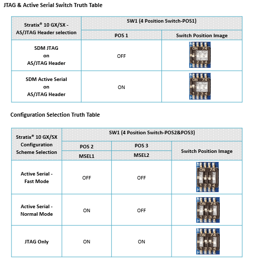
ブートスイッチ設定
オンボードスイッチ(SW1)が下図のように正しく設定されていることを確認してください。

デバッグポートの設定
Connect Type-A end of USB cable to PC and Micro-B end of USB cable to Development platform’s debug Micro USB connector(J13) as shown below.

Install the driver for Debug Port in Host PC/Laptop using the below link.
https://ftdichip.com/products/ft232rq/
JTAG接続
iW-RainboW-G45D Stratix10 GX/SX SoC FPGA SOM Development platform support JTAG interface for FPGA Programming and debugging. Use the USB Blaster to connect SOM.
Example USB Blaster which is tested with this Platform is mentioned below.
USB Blaster-2
Part Number : PL-USB2-BLASTER from INTEL
")
ヒートシンクの統合
iW-RainboW-G45D Stratix10 GX/SX SoC FPGA SOM Development platform comes with Heatsink+Fan attached to it. Make sure to power up the platform only with Heatsink+Fan attached.
Below is the Heatsink+Fan integration procedure for reference.


ヒートシンク+ファン
サーマルパッドステッカー

電源オン
Connect the Power supply plug to the Power connector (J10) of the Development platform as shown below and switch ON the power supply. Once power is applied to the Development platform, the power LED in the Development platform will glow as shown in the below image.

警告だ:
- Do not try to connect any other Power Supply other than supplied along with Stratix10 GX/SX SoC FPGA SOM Development Platform.
- Do not plug or remove the Stratix10 GX/SX SoC FPGA SOM from carrier board with live power.
- 電源LEDが点灯しない場合は、iWaveにご連絡ください。
テスト環境のセットアップ
前節で説明したように開発プラットフォームに電源が投入されると、開発プラットフォームに接続されている PC/Laptop のデバッグターミナルにブートメッセージが表示されます。すぐに端末のいずれかのキーを押してブート・ローダーのコマンド・プロンプトを表示するか、OSが起動するまで待ちます。OSが起動すると、デバッグターミナルにログインプロンプトが表示されます。ユーザ名とパスワードを "root "で入力すると、以下のようなLinuxコマンドプロンプトが表示されます。
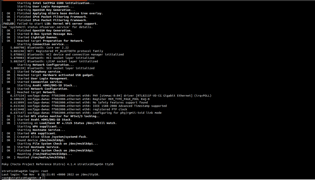
コマンドプロンプト